Intel: New Architecture To Sustain Moore's Law 'for Years to Come'
At a press event Wednesday, Intel revealed design improvements that will allow it to produce significantly faster chips with dramatically reduced power consumption.
Performance Versus Power Consumption
By re-architecting the transistor itself and moving to a tri-gate design, company representatives said, Intel will be able to shift to a 22 nanometer process (doubling transistor density) while at the same time boosting performance well beyond what it could have achieved with a 22 nm process using the older planar design found in its current 32 nm products.
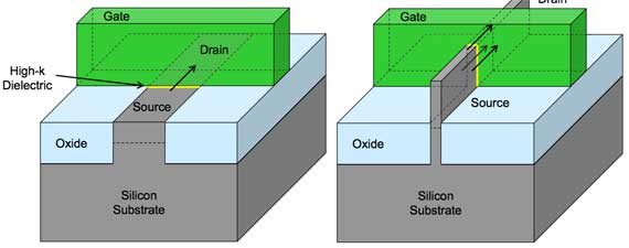
Planar versus "3D tri-gate" transistor design: The silicon "fin" in the new 3D design (right) allows for "fully depleted" operation, which provides greater performance gains at lower operating voltages. (Graphics provided by Intel.) |
This is especially true at lower voltages, where transistor gate delay can be reduced (and frequency increased) as much as 37 percent. Meanwhile, the new architecture also allows for significant cuts in power consumption--50 percent or more, according to the company.
Intel representatives at today's press event wouldn't comment on initial clock speeds or other specifications for chips using the new architecture but said simply those chips would be significantly more powerful while consuming significantly less power.
"The gains these transistors provide are really unprecedented," said Bill Holt, senior vice president and general manager of Intel's technology and manufacturing group, speaking at the press conference today. "We're going to be able to provide better performance and lower power at the same time and continue this on the historical pace and even improve it. These benefits will extend across our entire product line, from our highest-performance products to the smallest handheld devices."
Holt said the 3D tri-gate architecture, which has been in development for about 10 years, will allow Intel to sustain its historical pace of development following Moore's Law, which predicts a doubling of the number of transistors that can be packed into a given area on a chip every two years or so.
"This transition to 3D devices will help us continue Moore's Law," he said. "Clearly you can pack more things into the same space if you begin to go up as opposed to just sideways. So this will help us continue the scaling that drives the cost benefit."
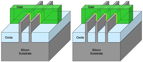
Multiple fins can be added to produce overall higher performance. (Graphics provided by Intel.) |
He said the new architecture will also take that even further with additional gains in the area of power savings.
"Moore's Law scaling and the march of technology has always provided a benefit in terms of active power reduction," he said. "The challenge in more recent generations has been continuing that. The fact is with this new 3D device we will actually increase the power savings that are available, more so than we've seen in past generations. So not only are we able to continue our traditional scaling, but we can actually provide an increased benefit in terms of active power reduction."
Intel senior fellow Mark Bohr explains the advances in the new 3D tri-gate design. |
2012: First End-User Devices?
The move to the 22 nm process is currently underway. Intel demonstrated working systems--a laptop and a desktop system--running on the "Ivy Bridge" architecture. Ivy Bridge is the successor to the Sandy Bridge microarchitecture used in current-generation Intel devices. The laptop Intel showed today was no more compact than notebooks currently on the market, but Dadi Perlmutter, executive vice president of Intel's architecture group, said the Ivy Bridge architecture could allow laptops to become "wafer thin."
Company representatives said Intel will be upgrading five fabrication facilities--two in Arizona, two in Oregon, and one in Israel--over the next one to two years to allow it to ramp up production, with the first end user devices possible as early as late 2012.
Chips will be designed initially for servers and other traditional computers. But the 22 nm process will also make its way into Atom-based SOCs (systems on a chip) designed for smart phones and tablets. Company representatives said they wouldn't discuss Intel's plans for the mobile/handheld device market at this point. But Intel senior fellow Mark Bohr pointed out that the new architecture results in "10 times lower [power] leakage," an important factor for handhelds, as well as "greater active power savings when set at a lower threshold voltage."
Detailed information about the new architecture can be found in a PDF document Intel prepared. It can be downloaded here.